


PCB processing industry laser processing solutions
-
Program overviewPrinted circuit boards are the foundation of electronic information products, so printed circuit board applications cover almost all electronic products, including communications and related equipment, computers and related equipment, consumer electronics, automotive electronics, aerospace electronics and other industries. Driven by the development trend of informationization and digitization, the PCB industry has broad market space and good development prospects. In
recent decades, the rapid development of integrated circuit technology and electronic information products has also driven the continuous advancement of printed circuit board technology. Printed circuit boards have evolved from single-sided to double-sided, multi-layer and flexible. Since a new generation of electronic products requires printed boards with higher density and more stable performance, high density and high performance are the future development of printed circuit board technology. As printed circuit boards move toward refinement, the use of lasers in the PCB industry is increasing. -
Program recommendation
PCB laser cutting
PCB is a patterned printed circuit board made of flexible substrate with high wiring density, light weight and thin thickness. PCB is mainly used in mobile phones, notebook computers, PDAs, digital cameras, LCM and other products, especially for applications with complex lines, high signal processing requirements or special electrical or mechanical performance requirements.
Disadvantages of traditional processing methods
For PCB cutting, the traditional processing method is to open the mold and then mechanically punch through the mold. This method of machining is a contact type of machining, so there are inevitably some shortcomings:
● Due to the increasing line density and pitch of PCB products, and the complexity of PCB graphics contours, it is becoming more and more difficult to make PCB molds. For a general PCB, it is difficult to make a mold, and the production cycle becomes long, which leads to a large increase in processing cost. For a PCB with high complexity, such a very complicated mold production cannot be realized, so it must be considered. A more advanced approach to cutting these complex PCBs.
● Due to the lack of machining itself, the PCB mold produced can not reach a high precision surface, which has a constraint on the further improvement of PCB processing precision. At present, the general mold processing can achieve an accuracy of ±50um, and it is very difficult or even impossible to achieve an accuracy of ±20um or less.
● Because the traditional PCB cutting process is a contact type machining method, it will inevitably cause processing stress on the PCB, which may cause physical damage to the PCB. At the same time, when the window is opened by the machining method, it is inevitable that the burr and the glue will be generated in the vicinity of the window, and the burr and the glue are after the bonding, pressing and the upper pad. Hard to remove, directly affecting the quality of the coating.
Advantages of laser processing
The working principle of PCB laser cutting machine is to scan the surface of PCB with 355nm ultraviolet short-wavelength laser beam, so that high-energy ultraviolet photons directly destroy the molecular bonds on the surface of flexible materials to achieve the purpose of removing materials. Ultraviolet laser processing belongs to “cold processing”. This “cold” photo-etched component has a small heat-affected zone with smooth edges and minimal carbonization to ensure the best quality of processed PCB products.
Dawn laser PCB laser cutting machine is a laser processing equipment integrating light, machine, electricity and material processing. Its processing advantages are obvious:
●The laser processing method is non-contact processing, and the heat affected zone of the component is small during processing;
● High Performance UV laser, small focus spot, uniform power distribution, small thermal effect, small slit width and high cutting quality;
● Precision 2D table and full-closed CNC system ensure fast cutting while maintaining micron order Accuracy;
● Position sensor and CCD image positioning technology, automatic positioning, focusing, making positioning fast and accurate, saving time and worry, high efficiency.


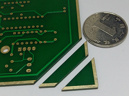
Dawn laser PCB board laser cutting sample Dawn laser PCB board laser cutting sample
PCB laser marking
Barcode tracing is an essential part of the production process of a circuit board. For the production management and defective product control, the manufacturer will use the bar code, text and other information to identify the product. At this stage, ink label paper is commonly used in the industry to paste on the product, but this method has many problems: large amount of consumables, high pollution, high labor costs, easy to remove marks. In response to this situation, the replacement of label paper by laser marking barcodes has become an industry trend.


PCB board laser marking sample PCB board laser marking sample